
Connector Engineering Guide
PCI Express Connector Pinout for Card Edge Selection
A PCI Express connector pinout assigns differential lanes, clock and sideband signals, power, and ground contacts across an add-in card and its mating slot. A generic diagram is only a reference. Before the PCB footprint is released, the link width, slot orientation, board-edge geometry, and supplier drawing must describe the same interface.
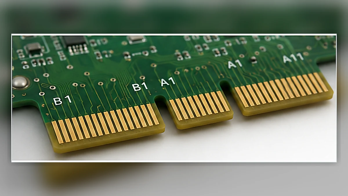
Engineering decision: treat the pinout as a controlled interface between the host schematic, endpoint documentation, PCB layout, and connector drawing—not as a library symbol copied from an unrelated design.
What the PCIe Pinout Controls
The pinout defines more than the high-speed lane pairs. It also places the reference clock, reset, wake, presence-detection, power, ground, and mechanically sequenced contacts. A mismatch in one group can prevent link training, reduce the available lane width, or create intermittent behavior that resembles a firmware fault.
Review signal names, polarity, and connector side before comparing physical appearance. Two parts that accept the same card shape can still differ in mounting details, contact geometry, keying, or drawing conventions. Mechanical insertion is therefore not proof of electrical compatibility.
PCIe Slot Types and the Review Focus
PCIe card-edge slots are commonly described as x1, x4, x8, and x16. The designation identifies lane width, but a longer slot does not prove that every possible lane is routed on the host board. The schematic and motherboard documentation remain the acceptance references.
| Slot | Lane width | Engineering review focus | Procurement check |
|---|---|---|---|
| x1 | 1 lane | Polarity, clock, reset, and presence signals | Confirm the exact footprint and slot orientation |
| x4 | 4 lanes | Lane order, return paths, and breakout routing | Check drawing revision and card clearance |
| x8 | 8 lanes | Complete lane mapping and reference-plane continuity | Confirm retention and insertion access |
| x16 | 16 lanes | Full assignment, mechanical fit, and system power review | Do not approve an alternate from catalog wording alone |
Format limitation: Mini PCIe, M.2, and other edge-card formats use their own mechanical and pinout definitions. Do not treat them as substitutes for a standard PCIe card-edge slot without a system-level comparison.
A Controlled Pinout Verification Workflow
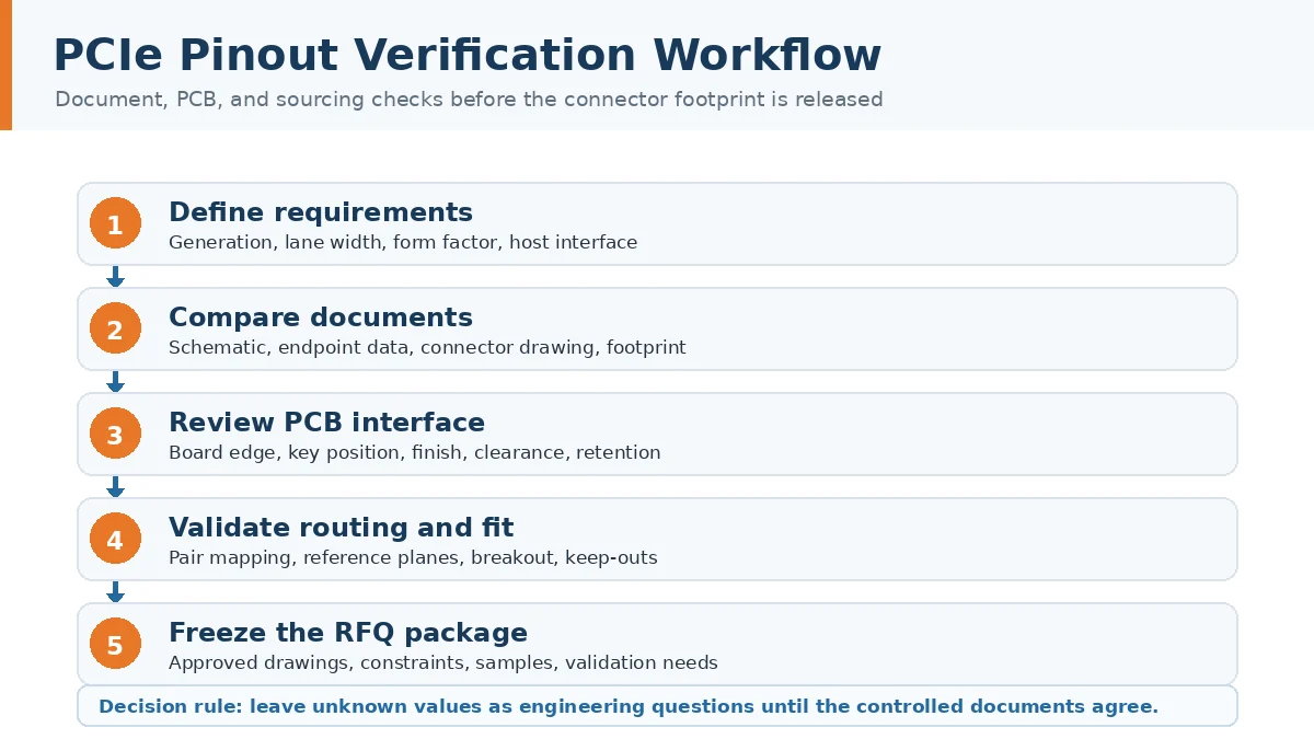
Pinout review is most effective when electrical, mechanical, and sourcing checks are completed in one sequence. Separating them can leave procurement with a connector that fits the board outline but does not match the released pad map or validation plan.
- Confirm the endpoint requirement. Record the required PCIe generation, lane width, card form factor, and host-board interface. State whether the design follows a standard add-in card definition or an application-specific edge card.
- Compare controlled documents. Cross-check the host schematic, endpoint documentation, connector drawing, and PCB footprint. Review polarity, sideband signals, grounds, key position, and slot orientation.
- Review the PCB interface. Confirm board thickness, edge-finger geometry, bevel, finish, insertion clearance, and retention method from approved drawings. These details affect contact engagement even when net names are correct.
- Validate routing and fit. Inspect differential breakout, reference-plane continuity, keep-out areas, and mechanical clearance. Simulation or a focused prototype should follow the project validation plan rather than being presented as a universal requirement.
- Freeze the RFQ package. Send the approved pinout, PCB and footprint drawings, stack-up constraints, mating information, sample expectations, and required validation records. Leave unresolved values as questions until the documents agree.
Failure Modes Worth Checking Before Release
Lane or polarity mismatch
Swapped assignments can stop link training or force operation below the intended width. Compare schematic net names with the endpoint documentation and the final PCB layout; do not rely on automatic naming conventions alone.
Sideband signal errors
Reset, wake, clock, or presence-detection errors may be diagnosed as software problems because the card still receives some power. Add these signals to the design-review checklist and verify their intended state at the physical interface.
Mechanical fit without electrical agreement
A card can enter a slot while routed lanes, keying, or system requirements remain incompatible. Acceptance should require both the mechanical drawing and the electrical assignment to match.
Uncontrolled connector substitution
Catalog descriptions do not establish identical contact geometry, finish, mounting, or qualification. Compare controlled drawings and decide whether an alternate needs footprint review, new samples, or revalidation before it enters the BOM.
Card Edge Connector Sourcing Checks
For PCIe and custom edge-card projects, the supplier review should cover contact count, key position, PCB interface requirements, finish, mounting, retention, insertion access, target environment, drawing revision, and the sample plan. Material, plating, flame rating, and test requirements should be treated as drawing- or application-dependent questions unless the approved product documentation states them.
LinkManu’s card edge connector family is a starting point for PCB edge-slot interface review. Final selection should follow the project drawings, mating information, and agreed validation scope.
Frequently Asked Questions
What is a PCI Express connector pinout?
It is the controlled assignment of lane pairs, clock, sideband, power, and ground contacts across the card edge and mating slot.
How do x1, x4, x8, and x16 pinouts differ?
They use different lane counts and therefore different numbers of differential pairs. Check the selected form factor’s electrical and mechanical documents.
Can a smaller PCIe card use a larger slot?
Some host designs allow it, but the routed lanes, motherboard support, endpoint, and firmware must be confirmed in the system documentation.
What belongs in the connector RFQ?
Include the pinout, PCB and footprint drawings, orientation, mechanical constraints, finish requirements, target environment, sample needs, and required validation records.
Send Your Connector Requirement
Share the drawing, BOM, mating information, target application, and open engineering questions. The review can then focus on connector fit, sample options, documentation needs, and RFQ readiness.