
Card Edge Connector Engineering Guide
How to Choose Printed Circuit Card Edge Connectors for B2B Projects
Knowing how to choose printed circuit card edge connectors starts with the PCB interface, not a catalog part number. A connector may appear suitable until the team compares the actual card thickness and tolerance, pad layout, insertion direction, retention method, electrical loading, operating environment, and expected service life. For a B2B project, those details should be agreed before samples are ordered or the footprint is frozen.
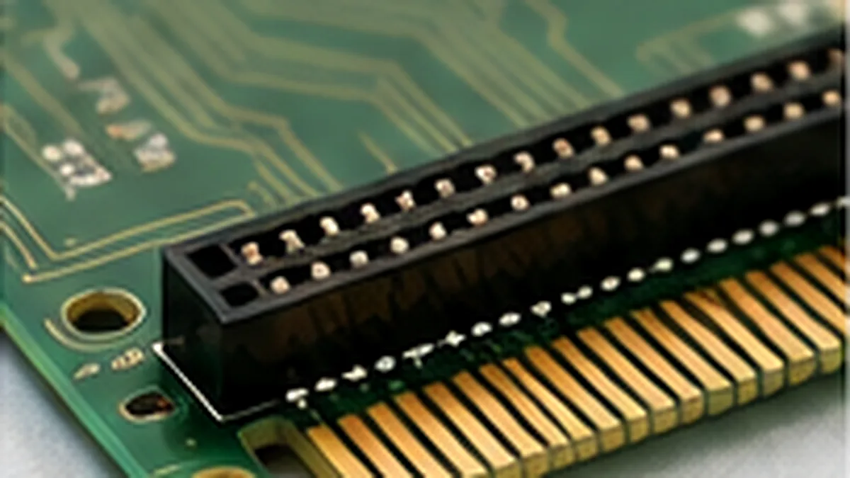
Engineering decision: do not approve the connector from pitch and position count alone. Confirm the complete mating interface and the conditions the assembly must tolerate.
Start With the PCB Interface, Not the Connector Family
The first review should compare the connector drawing with the PCB fabrication drawing. The board edge is part of the mating system, so a nominal match is not enough. Thickness tolerance, pad geometry, edge preparation, solder mask clearance, component keep-out areas, and card travel all affect whether the board enters the slot cleanly and reaches the intended contact position.
A purchasing description such as “card edge connector, same pitch, same number of contacts” leaves several failure paths open. Two products can share those headline attributes while using different card slots, contact locations, keying features, mounting details, or housing envelopes. Request an overlay or dimension-by-dimension comparison when the project is evaluating an alternative part.
| Interface item | What to confirm | Risk if omitted |
|---|---|---|
| PCB thickness and tolerance | Compare the finished board range with the connector card-slot requirement. | The board may be loose, difficult to insert, or outside the intended contact-force window. |
| Pad pitch, width, and location | Check the connector contact pattern against the released PCB artwork and drawing. | Contacts may land near pad edges or miss the intended conductive area. |
| Edge preparation | Confirm the required bevel or lead-in from the connector drawing and PCB fabricator. | Insertion force and contact damage risk can increase. |
| Keying and orientation | Verify key position, polarization, and the correct mating direction in the enclosure. | A mechanically possible reverse insertion can create an electrical fault. |
| Mounting and retention | Confirm board locks, latches, screws, standoffs, or chassis support required by the assembly. | Vibration or cable forces may be transferred directly to the solder joints and contacts. |
Drawing check: include the connector section view, PCB edge detail, mating direction, and nearby component envelope in the same review package. Separate drawings often hide an interference until the first assembly trial.
Separate Electrical Loading From Signal Requirements
The next decision is how each contact will be used. Power, ground, low-level sensing, control signals, and higher-speed links create different review questions. Do not assume a current rating or signal claim remains valid for the exact pin assignment, number of active contacts, enclosure temperature, and board layout used in your product.
For power contacts, ask for the conditions behind the published rating and decide whether temperature-rise verification is required with the planned pin map. For sensitive signals, compare contact resistance stability, return-path placement, routing geometry, and any available modeling or test documentation. Where impedance or crosstalk matters, the connector should be reviewed as part of the channel rather than as an isolated component.
- Power allocation: identify the contacts carrying load, the contacts used for return paths, and the contacts energized at the same time.
- Signal allocation: mark differential pairs, reference contacts, shielding needs, and any pins that require controlled sequencing.
- Abnormal conditions: state whether hot insertion, repeated service access, overload exposure, or operator misalignment is possible.
- Evidence required: define whether the decision needs a supplier data sheet, simulation output, sample measurement, or a formal test report.
The practical rule is simple: every critical electrical claim should have a stated condition and a document source. When that evidence is unavailable, keep the item open in the engineering checklist instead of converting it into an assumed specification.
Match Retention, Materials, and Environment to the Product Life
Mechanical retention should reflect how the card is installed and supported. A connector inside a stable enclosure may have different needs from one exposed to vibration, frequent maintenance, or chassis movement. Review the load path from the card to the connector, PCB, fasteners, and enclosure. The connector should not be expected to compensate for an unsupported card or poor alignment elsewhere in the assembly.
Material and plating decisions should also be tied to use conditions rather than selected by a generic label. Ask the supplier to confirm the terminal material, contact finish, housing material, and any required flame or environmental documentation against the drawing and end application. Expected mating activity, contamination, humidity, temperature cycling, and storage conditions can change what must be verified.
Procurement risk: a lower unit price is not a complete comparison when one option requires a PCB change, additional retention hardware, a new qualification cycle, or documentation that the supplier cannot provide.
Use Samples and Engineering Evidence Before Freezing the BOM
A sample is useful only when the team defines what it will prove. Fit checks should cover insertion, full seating, keying, clearance, retention, and removal. Electrical checks should reflect the intended pin assignment and loading. Environmental or durability testing should be planned only after the acceptance criteria and required documentation are clear.
Depending on project scope, supplier engineering support may include 3D modeling, housing-flow analysis, terminal stress analysis, or signal-integrity simulation. Some verification may be completed by the manufacturing source, while other tests may need to be arranged externally. Ask who performs each activity, which sample revision is tested, and whether the report will identify the exact connector and PCB configuration.
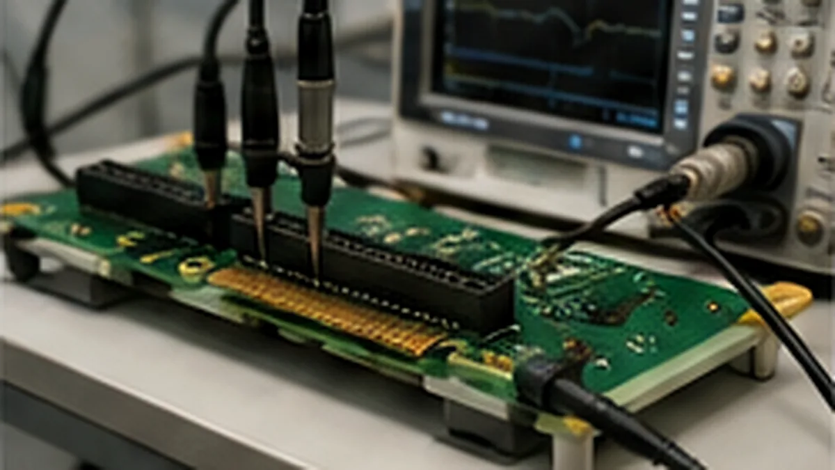
For a project-specific review, LinkManu can help organize drawing questions, sample requirements, and documentation requests before the final selection. Feasibility remains subject to the connector family, PCB interface, required processes, and evidence available for the project.
Build an RFQ Package That Allows a Real Feasibility Review
A useful RFQ gives engineering and sourcing teams enough information to identify mismatches early. Start with the PCB and assembly drawings, then add the electrical allocation, operating conditions, and commercial constraints. A photo or competitor part number alone is not sufficient for a compatibility decision.
| RFQ input | Decision it supports |
|---|---|
| Connector drawing or reference series | Defines the interface being evaluated and the dimensions that must be compared. |
| PCB edge detail and finished-board tolerance | Confirms card-slot fit, pad location, edge preparation, and insertion path. |
| Pin map and electrical use | Separates power, ground, signal, sequencing, and verification needs. |
| Assembly layout or 3D file | Checks housing envelope, component clearance, retention, and chassis alignment. |
| Environment and service expectations | Guides material, plating, retention, and test-document requirements. |
| Replacement or redesign boundary | Clarifies whether the footprint must remain fixed or controlled changes are acceptable. |
| Sample quantity, schedule, and approval plan | Aligns quotation timing with prototype, validation, and production-release gates. |
The LinkManu card edge connector product overview can be used to identify a starting family, but the final choice should still be confirmed against the drawing and application. Projects using rack-format hardware can also review the 3U card edge connector guide for format-specific questions.
Make the Selection Decision With Open Items Visible
Do not close the review because one sample mates successfully. Record which requirements are confirmed by drawing, which are supported by supplier documentation, which were checked on samples, and which remain assumptions. That record gives purchasing a defensible comparison and prevents an unresolved engineering question from being treated as an approved specification.
Before releasing the BOM, confirm the drawing revision, pitch and position layout, PCB thickness range, contact allocation, retention method, operating environment, expected mating activity, test documentation, sample result, and supplier capability for the required process. Any item without evidence should remain an action, owner, and due date.
Frequently Asked Questions
What is a printed circuit card edge connector?
It is a socket that mates with conductive contacts formed at the edge of a PCB. The PCB edge and connector must be reviewed as one mechanical and electrical interface.
Can pitch and contact count confirm compatibility?
No. Also compare board thickness, pad location, keying, housing dimensions, mounting, mating depth, and electrical use.
What should procurement send for a replacement review?
Send the original drawing or data sheet, PCB edge drawing, photos, pin map, sample if available, and a clear statement of which dimensions cannot change.
When is sample testing necessary?
Use samples when fit, insertion, retention, electrical loading, or documentation cannot be confirmed from approved drawings and data alone.
How should an alternative connector be approved?
Approve it against a documented comparison, sample results, required reports, and the released PCB and assembly revisions—not only a cross-reference statement.
Send Your Connector Requirement
Share the connector drawing or reference, PCB edge detail, pin map, application environment, sample needs, and documentation requirements. These inputs allow a focused feasibility review before quotation or BOM release.

Technical content reviewed by LinkManu Engineering Team
Prepared by LinkManu Editorial Team for B2B connector engineers, sourcing teams, and product development projects. Updated 2026.