
Board-to-Board Connector Engineering
How to Select a Board-to-Board Mezzanine Connector for a PCB Stack
A mezzanine connector should be selected from the assembled PCB stack, not from pitch and pin count alone. The drawing must show the real board-to-board distance, component keep-outs, mounting points, and the direction in which the boards are mated. Procurement can then compare connector families without separating mechanical fit from electrical and production requirements.
This board to board mezzanine connector selection guide focuses on the decisions that belong in an engineering review and RFQ. Any rating, material, plating requirement, or test condition still needs confirmation against the supplier drawing and the end application.
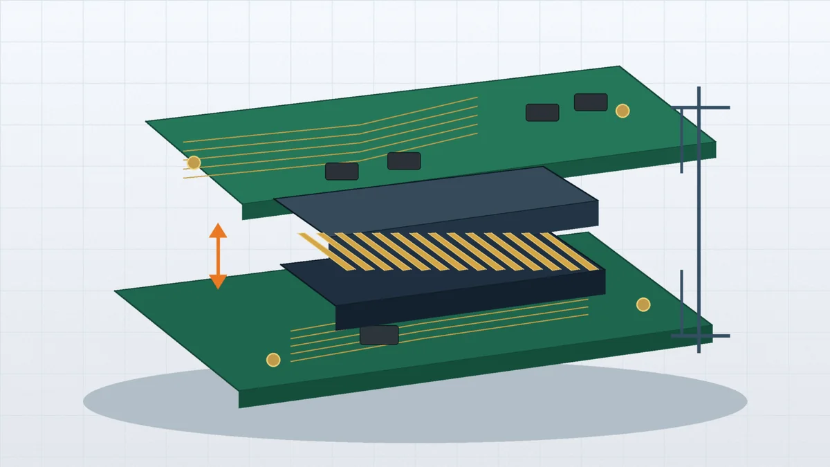
Engineering decision: Freeze the board stack and acceptance criteria before asking for a connector quotation. A part number selected before the mechanical model is stable usually creates another review cycle later.
Start with the PCB Stack, Not the Connector Catalog
The target mating height must come from the mechanical model. Include both PCB thicknesses, standoffs, fasteners, nearby component height, enclosure constraints, and expected board deflection. The connector should not be used to pull two misaligned boards into position unless the selected design is intended to absorb that offset.
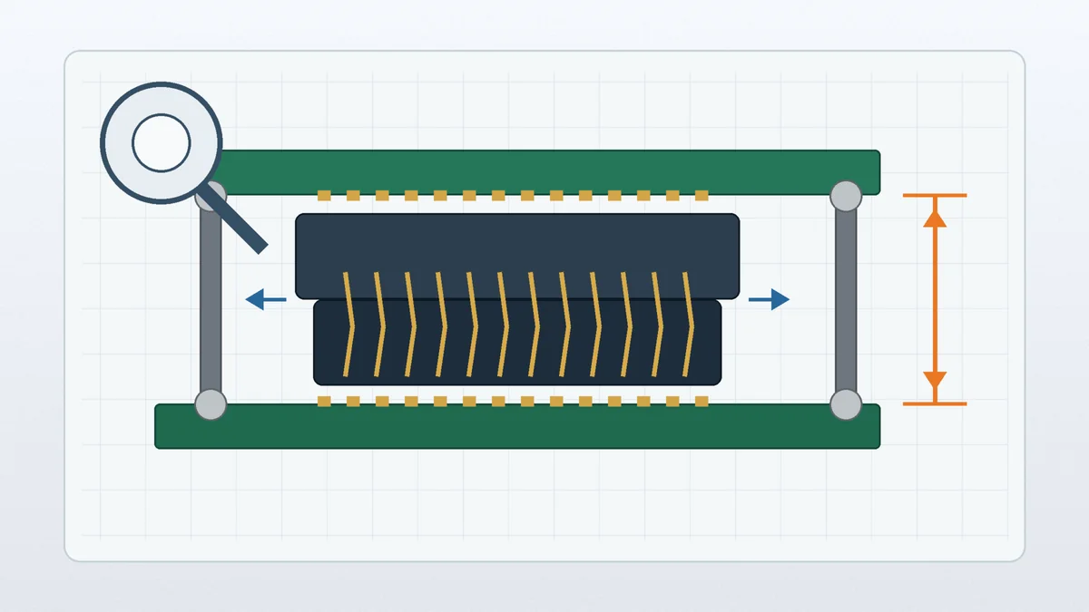
Build a tolerance loop before choosing the plug and receptacle combination. The loop should cover PCB thickness variation, connector dimensional tolerance, mounting-hole position, housing seating, and any fixture or enclosure load applied after assembly. Reject a candidate when the worst-case stack can bottom out, lose contact engagement, or place side load on the connector housing.
Questions to settle in the mechanical drawing
- What is the required fully mated board-to-board distance?
- Which board is fixed, and which board can move during assembly?
- Is the mating path vertical, side-entry, or constrained by the enclosure?
- Are hold-downs, locating pegs, keys, or additional board supports required?
- What misalignment remains after the PCB and enclosure tolerances are combined?
Build the Selection Matrix Around Failure Modes
A useful comparison sheet does more than list catalog specifications. It shows what the project needs, how that requirement will be checked, and what would disqualify a candidate. This keeps engineering, sourcing, and quality teams working from the same acceptance criteria.
| Review area | Evidence to request | Reject or rework the choice when |
|---|---|---|
| Stack height and engagement | Dimensioned connector drawing, mated cross-section, sample pair | The worst-case PCB stack leaves uncertain engagement or housing interference |
| PCB retention | Footprint, hold-down or peg details, assembly recommendation | The connector relies on solder joints to carry avoidable mating or side load |
| Signal assignment | Pin map, return-path plan, project-specific electrical review | Power, ground, and sensitive signals cannot be routed with an acceptable layout |
| Operating environment | Material and plating information plus agreed test conditions | The supplier cannot confirm the required environment or documentation |
| Supply continuity | Lifecycle status, tooling ownership, sample and production lead-time basis | The program depends on an unverified source with no change-control plan |
Use Pitch and Connector Style as Layout Constraints
Pitch affects routing space, pad breakout, inspection access, and the amount of alignment error the assembly can tolerate. A smaller pitch is not automatically the better choice. The PCB designer should confirm that the footprint, via strategy, solder-mask definition, and inspection method are realistic for the intended process.
The supplied product references for this article include a 66A2 power-and-signal floating board-to-board connector at 0.50 mm pitch, a 66C8 floating reference at 0.80 mm pitch, and a 66H3 anti-misplug reference at 2.54 mm pitch with listed pin options from 06 to 100. These are family-specific examples, not a promise that every pitch, pin count, or mating height is available. Final feasibility should be confirmed from the drawing, sample, and application requirements.
For a wider product-family review, see Board-to-Board Connectors for Compact PCB Interconnects. Use the category page to identify candidate styles, then return to the project drawing before selecting a part.
Confirm Electrical and Environmental Acceptance Before Sampling
Electrical review must be based on the actual pin assignment and operating condition. Do not multiply a per-contact rating by the number of parallel pins and treat the result as guaranteed capacity. Current sharing, copper distribution, temperature rise, contact resistance, and adjacent loaded positions must be reviewed for the proposed layout.
- Define the circuits. Separate power, ground, low-speed control, and any high-speed or impedance-sensitive signals.
- Request the relevant ratings. Confirm current, voltage, contact resistance, insulation resistance, material, plating, and flame-rating requirements for the exact part.
- Match the test plan to the application. Specify whether insertion/extraction force, temperature rise, hi-pot, impedance, humidity, vibration, salt spray, or other environmental checks are required.
- Set acceptance limits before testing. State what change in resistance, mechanical damage, housing movement, or signal performance would fail the sample.
- Confirm documentation. Ask which reports can be supplied, which tests may be arranged externally, and which checks are project-dependent.
Risk check: A generic qualification report may not represent your pin loading, PCB stack, mating height, or environment. Link the requested evidence to the exact connector and test configuration.
Compare Part Price with Program Risk
Piece price matters only after the connector can be assembled, tested, and supplied consistently. Compare the total commercial effect of each candidate: PCB layer or routing impact, placement and inspection difficulty, additional fixtures, expected rework, sample lead time, tooling needs, and the cost of changing the layout after validation.
Procurement should also ask who controls the tooling, how drawing revisions are approved, what minimum order assumptions support the quotation, and how material or plating changes are communicated. A lower quoted unit price can be the wrong decision when it creates a single-source dependency or requires a more expensive PCB process.
Prepare an RFQ Package That Can Be Reviewed
An RFQ should allow the supplier to judge fit and risk without guessing. Send enough information to evaluate the connector pair, but keep the package focused on the interface rather than the full product design.
| RFQ item | What the supplier should confirm |
|---|---|
| Dimensioned PCB cross-section | Target mating height, clearance, board thickness, and mounting relationship |
| Pin count and circuit allocation | Feasible family, contact arrangement, and any mixed power-and-signal requirement |
| Footprint or interface drawing | Pad layout, orientation, retention features, and mating direction |
| Environment and validation plan | Required materials, documentation, test scope, and acceptance criteria |
| Program information | Sample quantity, forecast range, schedule, customization boundary, and change control |
Sample review before BOM release
- Check the supplier drawing against the current PCB and enclosure model.
- Build the exact plug-and-receptacle pair on representative boards.
- Inspect seating, alignment, solder joints, connector retention, and nearby component clearance.
- Run the agreed electrical and environmental checks with documented pass/fail limits.
- Release the BOM only after the drawing revision, sample result, and production footprint match.
When to Request Floating or Custom Review
A floating connector may be worth reviewing when the board pair has residual assembly offset that cannot be removed economically through fixture, enclosure, or PCB changes. It is not a substitute for an uncontrolled tolerance stack. The allowable movement, mating force, retention, and test conditions still need confirmation for the selected family.
Projects requiring tolerance absorption can start with Floating Board-to-Board Connectors. Request a semi-custom or custom feasibility review when the required mating height, orientation, keying, pin grouping, or combined power-and-signal layout cannot be met by an existing family. Company materials provided for this article list Pro-E modeling, Moldflow analysis, ABAQUS terminal stress analysis, and SI simulation as project-dependent engineering tools; the applicable work should be confirmed in the RFQ rather than assumed.
FAQ
What should be confirmed first for a mezzanine connector?
Confirm the fully mated board-to-board distance, mating direction, pin allocation, and remaining assembly misalignment.
Can pitch alone determine the right connector?
No. Pitch must be reviewed with routing, stack height, retention, electrical requirements, and assembly capability.
When is a floating connector appropriate?
Review one when controlled residual PCB offset remains after the mechanical tolerance loop is complete.
What should be included with the RFQ?
Send the interface drawing, PCB cross-section, pin plan, environment, test requirements, sample quantity, and schedule.
Next Step: Freeze the Interface Before Quotation
Prepare the current drawing, target mating height, pin assignment, operating environment, validation requirements, and expected sample schedule. These inputs let engineering and sourcing compare connector options on the same basis and identify whether a standard, floating, semi-custom, or custom review is appropriate.
Send Your Connector Requirement
Share the PCB interface drawing, stack height, pin plan, application conditions, and required documentation for project review.

Technical content reviewed by LinkManu Engineering Team
Prepared by LinkManu Editorial Team for B2B connector engineers, sourcing teams, and product development projects. Updated 2026.